Friday, 30 November 2012

WOW!!!CANON...


27 NOVEMBER 2012, TUESDAY....We, all of the Electronics System Engineering students having a very nice visit to CANON factory that placed at JALAN SELISIK, SEKSYEN 26, 40400 SHAH ALAM, SELANGOR DARUL EHSAN. 
On that day, we arrived at the factory after one hour finding the factory...hehe...When we arrived, we saw some CANON's employee were waiting for us at the front door of the factory...so sweet...and we having some time to take some picture together as a memory.
After that, we are forwarding to a hall for some briefing and talk. First thing that briefed to us is about the safety precaution that we have take during the visit. This briefing was given by the representative from Safety and Health Department. After finished the briefing, there is another representative from the CANON that give us the talk about the company profile.
Started from year 1988, the company was build and the company was opened during year 1991. Up until now...there is a lot of achievement that they have done. One that is most great achievement is during year 1993 where they have received a National Landscape Awards Champion in Industry Category. 


The briefing was finished, and now we are forwarding to visit the water treatment area. During the visit, the person who accompany us tried to explain to us about how they handled their waste after the production. The production of the camera used so many water in order to make the camera. Therefore, to sustain the environment, they have build some building that placed many tank that needed to treat the water. They used a MEDIA FILTER to remove a fine particles from the water. They also used the process of REVERSED OSMOSIS to remove the minerals. After the water have treated, 45 percent of the water were used back for the production.


NOW, the time that we have been waiting for, visiting the production of the camera area. Firstly, we have to cover up our feet with some kind of plastic to prevent the dirty from our shoes affecting the process of camera production. During the visit, Mr Nor Mohammad as the manager at the factory was accompanied us. There is a lot of things that he told us.  About the production, products that they have produced and some other things about the factory. From the visit, I realized about something. Engineers not only responsible to design some products that will improve our economy but also at the same time have to think about the affects that we will produced to our environment. And think of some other way to reduce the effect. So, GOOD LUCK TO US AS BECOMING ENGINEERS. :)


Saturday, 24 November 2012

ELECTRONIC SYSTEMS IN INDUSTRY :D

Tuesday, 20 November 2012....SMJE students had attend a talk about 'Electronic Systems in Industry'. This talk presented by Mr. Vivek Panicker, who is the Excecutive Director of Titan Thermal Solutions.

In the two hours talk, we have heard many inputs given by Mr. Vivek. He start the talk with the Overview of Electronic System. During this time, we all have been told about the definition of electronics and electronic system.


ELECTRONICS : ELECTRICAL CIRCUITS THAT INVOLVE ACTIVE ELECTRICAL COMPONENTS SUCH AS VACUUM TUBES, TRANSISTOR AND DIODES.

ELECTRONIC SYSTEM : GROUPINGS OF ELECTRONIC CIRCUITS AND COMPONENTS WHICH ARE DESIGNED TO ACCOMPLISH ONE OR MORE COMPLEX FUNCTIONS.

Mr. Vivek also explained to us more about electronic systems. Electronic system is fundamental to our daily life. It also played a key role in advancement of technology. In addition, it will be a mainstay in future development.

Other than that, he also have show us the progression of the electronic system. You can see from the following :


1. Large =====> Small =====> Miniature

2. Simple =====> Complex Architecture

3. Analog =====> Digital

The SECOND thing that he told us is about the 'Role of Electronic in Industry'. I will simply jot it down in a point form :~

1. Vital to current information and technology era.
2. Penetrated seamlessly through various industries.
3. a catalyst to enhanced production and productivity within industry.
4. Most industries today are heavily dependent on it for their daily operations.

The electronics also conventional classified into :~
1. Consumer.
2. Industrial.
3. Defense.
4. Communication.
5. Information Processing System.

The important thing that we should know about electronic is that it plays two crucial parts in industry, as a platform for development or design of new systems and as a means to increase productivity of current systems.

Next, we should go through the IMAGING INDUSTRY WORLD...

Imaging is the representation of an objects outward form.


CHEMICAL IMAGING ==> SIMULTANEOUS MEASUREMENT OF SPECTRA AND PICTURES.

DIGITAL IMAGING ==> CREATING DIGITAL IMAGES, GENERALLY BY SCANNING OR THROUGH DIGITAL PHOTOGRAPHY.

GEOPHYSICAL IMAGING ==> SATELLITE.

MEDICAL IMAGING ==> CREATING IMAGES OF THE HUMAN BODY OR PARTS OF IT, TO DIAGNOSE OR EXAMINE DISEASE. 
                            
MOLECULAR IMAGING

OPTICAL IMAGING

RADAR IMAGING ==> FOR OBTAINING AN IMAGE OF AN OBJECT, NOT JUST ITS LOCATION BUT ALSO SPEED.

THERMOGRAPHY ==> THERMAL IMAGING

The advent of electronics have moved the imaging into new heights. This leads the development of new methodologies. Imaging technology have moved into new wavelength spectrums for commercial usage.

Now, we move on the 'Basic Concepts and Terms of Imaging'....

@ PIXELS AND RESOLUTION
     ~ A digital image is formed by pixels.
     ~ Smallest piece of information in an image.
     ~ Often represented using dots, square or rectangles.
     ~ More pixels in an image, the sharper and clearer the image is.

@ VIDEO AND FRAMES
     ~ A digital stream of video is made up of a group of pictures (Frames) captured across a period of
        time.
     ~ More frames per second, the lesser the jitter in the video.

@ NTSC AND PAL
     ~ Human eye require a minimum 25 frames a second.
     ~ PAL TV standard :-
                  - 25 frames per second
                  - Resolution of 320 by 720
                  - Asia, Europe, South America and East Africa
     ~ NTSC TV standard :-
                  -30 frames per second
                  - Resolution of 480 by 720
                  - North America and Japan

Imaging industry requires processing huge quantities of data in a short span. Electronics eases these complexities, making the technology affordable.

ELECTRONICS WITHIN THERMAL IMAGING INDUSTRY
^.^  Thermal imaging originally a spin-off defense electronics.

^.^  Makes use of wavelength in 7-14 micrometer to form an image.

^.^  Sensors make use of focal plane arrays and are commonly Indium Gallium Arsenide (In Ga AS).

^.^  Often referred to as a 'Dirty Imaging System' compared to CCD and CMOS architectures.

^.^  A lot of pre and post processing of data is required.

^.^  Thermal requires Non-Uniformity Calibration (NUC) on data stream.

^.^  Data varies in state and space.

^.^  Enables implementation of intensive algorithms such as Kalman Filters, Edge Detection and 
       Neural Network Modeling.

^.^  Incident Energy(I) = Emitted Energy(E) + Transmitted Energy(T) + Reflected Energy(R)

^.^  Equations are expanded into models that are described in electronics.

^.^  Electronic processing data allows thermal imaging to be used in various other industries :-
       1) Maintenance
       2) R&D
       3) Medical research

^.^  Electronics and the advancement of technology has huge impact on thermal industry.

Friday, 9 November 2012

REFLECTIVE JOURNAL 4

Hmm...I wonder what should I write in this entry since I'm not there in the public lecture. I do not why suddenly I got dengue that time....huhu....really depressing. I do really want to attend the lecture so that I can also hear about the experiences Dr Azran had at Japan. Hearing it from my friends makes me feel really disappointed that I can not attend the lecture.

Now I want to describe a little about bioelectronics. We can define bioelectronics as a branch of science that deals with electronics control of physiological function especially as applied in medicine to compensate for defects of the nervous system. We can also simply said that bioelectronics is a branch of science that deals with the role of electron transfer in biological processes.

Wah...that is what I got from Mr Google....huhu....Even I am not attend the lecture but I have to take note about it right???

Another thing that my friend tell me about the lecture is doppler effect...which included in Dr Azran research project.

DOPPLER EFFECT is an increase or decrease in the frequency of sound waves as the sound-producing object moves toward or away from an observer. The most popular example of doppler effect is AMBULANCE SIREN....

  • as ambulance approaches, the siren's sound waves become more frequent.
  • as the ambulance drives away, the siren's sound waves become less frequent.
  •  
Example of doppler effect
    The students also were told about how to calculate IMPEDANCE....
That is all for this time....see you guys on the next entry....

Sunday, 28 October 2012

ALL ABOUT ULTIBOARD :)

What is ULTIBOARD??? 


 ULTIBOARD is......
the PCB layout application of National Instruments Circuit Design Suite that assists us in carrying out the major steps in the circuit design flow. Ultiboard is used to design printed circuit boards, perform certain basic mechanical CAD operations and prepare them for manufacturing, It als provide automated parts placement and layout.

There are many procedure using the ULTIBOARD...You can read it and think for a while how to use it.
NUMBER ONE :~
Open the saved circuit file from the Multisim and transfer the schematic design to Ultiboard 10 by selecting Transfer >> Transfer to Ultiboard 10.


NUMBER TWO :~
Use the Save As dialog box to save the new ultiboard file to your Z drive. Click OK on the message box that appears.
NUMBER THREE :~
Accept the default trace width and clearance that is given when Ultiboard opens. Make sure that all fields are selected in the Import Netlist Action Selection window and click OK.
NUMBER FOUR :~
Select the Layers tab near the middle of the left of the screen. This lists the board layers and other useful elements of the board. Double clicking a particular layer sets that layer as active. Double click Board Outline from the list.
  NUMBER FIVE :~
Right click an edge of the yellow rectangle and select Properties from the menu that appears. Under the rectangle tab set the width to 2000 and the height to 1500. Click OK and notice that the yellow rectangle become much smaller. This rectangle represents the area of the circuit board in which all of the components and traces must fit.
NUMBER SIX :~
The next step to PCB design is to layout the components. Double click the checkbox next to Ratsnest in the layers list. This remove the yellow lines that connect all of the components together and simplifies the picture.
NUMBER SEVEN :~
Begin placing the components inside the yellow rectangle. Notice single brown lines coming out of each component. These are Force Vectors and they point to the most efficient place to put the component based on its necessary connections. Use this as a guide for placement, but be careful because Force Vectors would ideally have all of the components stacked on top of each other in the middle of the board.
NUMBER EIGTH :~
The next step is setting up the routing parameters for laying out the copper trace. Go to the Netlist Editor by selecting Tools >> Netlist Editor. This tool keep track of all connections between pins on the board. Each set of pins connected together are referred to as a Net. Use the dropdown menu in the Netlist Editor to view the different Nets n the board. The tabs in the Netlist Editor provide different information and option for the selected Net.
NUMBER NINE :~
To prepare the Nets for routing select the first Net from the list. Select the Misc tab and check the box next to Copper Bottom. This tells the Autorouter that this Net can be connected by palcing trace either on the top of the board or the bottom of the board.
NUMBER TEN :~
In this case it is the best if the Autorouter can use the top or bottom layers for all of the Nets. To save times select the Nets tab from the group of tabs at the bottom of the screen. Right click one of the rows and choose Select All from the menu that appears. Click inside one of the cells in the Routing Layers column. Check the box next to the Copper Bottom in the window that appears and click OK
NUMBER ELEVEN :~
The board layout is ready for the Autorouter. Start the Autorouter by selecting Autoroute >> Start/Resume Autorouting. The Autorouter should only take seconds to place traces on the board. Notice that there are green and red lines that appear. The green lines represents copper trace on the top layer of the board and the red lines represents the copper trace on the bottom layer f the board. 


NUMBER TWELVE :~
It is important to cleanup and check the work of the Autorouter after use. Excessive bends and sharp angles in the traces greatly increase the chances of board failure during manufacturing and use. Take some time to look through the traces and get a feel for dragging traces into more appropriate shapes and angles. The Autorouter is never perfect and there are always traces that can be cleaned up.
NUMBER THIRTEEN :~
Once you are satisfied with the traces on the board Save and Close the design.

And one more thing that attracts me is the this program will show us the 3D figure of the circuit that we designed. Awesome!!!!


Thats all...I hope everyone will take some time to read this entry...ARIGATO!


Monday, 8 October 2012

CIRCUIT ON COMPUTER????THINK ABOUT IT....

 MULTISIM AND A LITTLE INFORMAION ABOUT ULTIBOARD...
HOPE YOU GUYS LIKE IT!!!

Ehem...Ehem....
Here is the new entry....

In this entry I will tell you guys about my recent Introduction to Electronics System class.
On that day all of section 2 students have to go to the Electronics Workshop.
There is a lot of computers in that workshop but not all of the computers can working.

First thing that we do in the workshop is we are briefing by Dr. Kamal about the assessment on the reflective journal that we have to do every week.
There are some papers that have been distributed to us.....

First...
OVERALL ASSESSMENT CRITERIA

 On this paper, there are the criteria that students need to follow to get good result. 
In this subject, the thing that will be judge is the reflective journal, practical, presentation and also attitude.


THE SECOND THING THAT WE GOT...

Dr.Kamal mostly focus on the reflective journal that day. This is because many of the students do not really understand what actually needed to write in this journal.
Because of that Dr. Kamal give us the booklet explaining about the reflective journal.

Actually, there is a lot thing that Dr. Kamal has given to us but I think I should stop here and start
writing about the second session in this class which taken over by Mr. Redzuan...

In this session, we are learnt about construct a circuit in a computer.
The software that we use are  NI Multisim 10 and also Ultiboard.

FIRSTLY, I WILL TELL YOU GUYS ABOUT THE MULTISIM...
NI MULTISIM 10!

When you enter this software, you can see an empty space which specially design for the user to construct a circuit on it.

THE EMPTY SPACE FOR DESIGNING THE CIRCUIT

Let I explain a little about the Multisim. This software integrates two programs that is a circuit schematics editor and a circuit simulator. The schematics editor allows us to build a virtual circuit by connecting various electronics components. Basically the user draws the schematic of the circuit to be analyzed. 

Before we start constructing the circuit. We are given a simple schematic diagram that we have to design in the software.

THE SCHEMATIC DIAGRAM THAT GIVEN TO US.
 Mr Redzuan teach us how to use the software before we try it by ourselves.
He explained the whole thing about how to construct the circuit in the software.

MR REDZUAN AT THE FRONT EXPLAINING ABOUT THE SOFTWARE.
The first thing we have to know is the toolbar.

THE TOOLBAR
From the toolbar, we can choose the icon that we need.
Here, in the menu icon, we can choose the components selection menu.
In this menu, we will choose the components that we need. 
We also can get the components icon just by clicking the left button of the mouse.

THE COMPONENTS SELECTION MENU

In the Component Selection Menu, set “Database” to “Master database” and “Group” to “Sources.”
 We can choose the type of the components and the value of the components from here. After that, we can just connect the components by a wire.

THE CIRCUIT THAT HAVE DONE
 Alhamdulillah...
I already finish constructing my circuit...
And alhamdulillah again when I RUN it, it does work.
The LED did lighted.
FUHH....

But one more thing that I forget....
From the picture, we can see there are some symbol of the components have blue colour while the others is black.
Actually, the components with blue colour represent the real components while the black colour represents the virtual components. When the circuit in the Multisim software imported to the Ultiboard software, only the real one will be appear there whereas the virtual one cannot appear in the software. In this case, we need to change the components type in order to complete the circuit in the Ultiboard. Just double clicking on the components in the Multisim and choose the real one. And then the components will appear in the Ultiboard circuit.
But, be careful. Make sure that the value of the components are the correct one.

I think thats all....
We are not done yet with the Ultiboard...
Therefore, I will stop here and will comeback soon with more story on Ultiboard...
BYE2...


Friday, 5 October 2012

COMPONENTS.. :)


COMPONENTS.....

Assalamualaikum...
             Arigato gozaimasu....               
Hehe...
And...Happy Reading....

 In this entry, I would like to show many components that we, SMJE students have learnt before with Mr Redzuan. Hmm...actually, I am a little bit suprise because our lecturer have been changed that day. Where is Dr. Kamal???All of the students keep wondering about it. We are waiting untill Mr Redzuan tell us about the truth that he will teach us for seven weeks and after that the lecturer will be change again...Hmm...Interesting...

Back to our topic...
COMPONENTS!

We are given many components on that day...AND
The FIRST COMPONENT IS...

RESISTOR

there are two types of resistor :~
Through Hole Resistor


 and

SMD Resistor
 That day, we are not only study about the physical of resistor. We also study about how to calculate the value of resistor by their colour code.

The table in FIGURE 2 shows the colour that represents certain value. This color code will help us to calculate the value of the resistor. As we know, the resistor have their own specific color. We just have to know what the color and the value represent by the color. Then we can calculate it by a simple calculation.

Value of resistor based on color code calculation
That is for through hole resistor...
For SMD resistor...
They have their code on their body...
As you can see before, the picture...
Now, the difference in determining the value of SMD resistor...

The way to determine the value of SMD resistor

See the picture carefully, we can see that SMD resistor use some code represent their value. We can determine the value by their code on their body.

Now, the SECOND COMPONENT IS....

CAPACITOR

here are TH CAPACITOR and SMD CAPACITOR:~

This is through hole capacitor
 
Capacitor is differ from resistor...capacitor did have negative and positive terminals...we can determine the polarity by the legs and also body...

Negative and positive terminals
From the above picture, it shows that the shorter leg represents the negative terminal and the long one represents the positive terminal.

Negative and positive terminals

From the above picture, we can determine that at the grey colour side on the capacitor's body represents the negative terminal.

SMD CAPACITOR


The above figure show the other type of capacitor...which is SMD Capacitor.


SMJE STUDENTS ALSO HAVE LEARNT ABOUT THE WAYS TO DETERMINE THE VALUE OF CAPACITOR

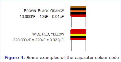
The first thing, the value of capacitor can be determine by the color code same as resistor but there is some differences between them.

Capacitor color code
Diagram of capacitor
The three figure above show the table of color code, the diagram of capacitor with specific color and also how the we can get the value of capacitor by their color code.

The SMD CAPACITOR also have their own speciality in determining their value. We can determine their value by the code presented on their body.

This is the example of how we can determine the value of SMD CAPACITOR by their code.

Overall, exactly, the value that we determine is not the accurate value of the components. We can have the accurate value of these components by using the multimeter.

Digital Multimeter
The above figure shows the example of multimeter that is used to get the actual value of components.

Hmm...I think thats all that I can share with you guys...
Hope this entry will give some knowledge to you all....
And also as a reminder for me...
Hehe...
See you guys in the next entry..
TATA